
Accueil > Équipes scientifiques > Surfaces, Interfaces, Molecules & 2D Materials (SIM2D) > Matériaux à grand gap : Diamant, Carbure de Silicium et Oxydes
Matériaux à grand gap : Diamant, Carbure de Silicium et Oxydes
Transparent wide band-gap materials play a crucial role in many applications ranging from high power micro-electronics, and opto-electronics ranging from photo-voltaic cells to photo-catalysis. For Diamond, Silicon carbide and oxide materials to be used in nanoscale applications, several challenges must be overcome. These include surface preparation, atomic-scale characterisation, efficient doping, conductivity and molecular adsorption.
Techniques : UHV NC AFM - RT STM - LEED - H Plasma - Atomic Layer Epitaxy (ALE)
Matériaux à grand gap - Diamant, Carbure de Silicium, et Oxydes
Diamond & Silicon Carbide
Leader : Andrew Mayne Participants : Hamid, Oughaddou, Hanna Enriquez, Gérald Dujardin Students : Past Contributors : Geneviève Comtet, Tamara Ovramenko, Heejun Yang, Guillaume Baffou Surfaces of wide band-gap semiconductors are expected to play a crucial role in many applications ranging from high power micro-electronics, photo-voltaic cells to photo-catalysis. Transparent silicon carbide and diamond surfaces are also ideal for atomic-scale opto-electronic experiments. However, the use of these wide band-gap semiconductor surfaces for molecular nanosciences poses a number of problems such as surface preparation and atomic-scale characterisation, efficient doping, conductivity and adsorption of molecules. |

Techniques : UHV NC AFM - RT STM - LEED - Hydrogen Plasma - Atomic Layer Epitaxy (ALE)
Highlights
|
article : A. El Boujlaidi, N. Rochdi, M. R. Tchalala, H. Enriquez, A. J. Mayne, H. Oughaddou, "Growth and characterization of nickel oxide ultra-thin films", Surfaces & Interfaces 18, 100433 (2020)
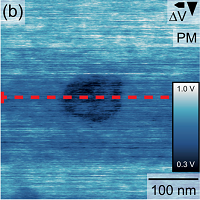 Kelvin probe force microscopy studies of the charge effects upon adsorption of carbon nanotubes and C60 fullerenes on hydrogen-terminated diamond. Hydrogen-terminated diamond is known for its unusually high surface conductivity that is ascribed to its negative electron affinity. In the presence of acceptor molecules, electrons are expected to transfer from the surface to the acceptor, resulting in p-type surface conductivity. Here, we present Kelvin probe force microscopy (KPFM) measurements on carbon nanotubes and C60 adsorbed onto a hydrogen-terminated diamond (001) surface. A clear reduction in the Kelvin signal is observed at the position of the carbon nanotubes and C60 molecules as compared with the bare, air-exposed surface. This result can be explained by the high positive electron affinity of carbon nanotubes and C60, resulting in electron transfer from the surface to the adsorbates. While the presence of a charged adsorbate or a difference in work function could induce a change in the KPFM signal, a charge transfer effect of the hydrogen-terminated diamond surface, by the adsorption of the carbon nanotubes and the C60 fullerenes, is consistent with previous theoretical studies. Kelvin probe force microscopy studies of the charge effects upon adsorption of carbon nanotubes and C60 fullerenes on hydrogen-terminated diamond. Hydrogen-terminated diamond is known for its unusually high surface conductivity that is ascribed to its negative electron affinity. In the presence of acceptor molecules, electrons are expected to transfer from the surface to the acceptor, resulting in p-type surface conductivity. Here, we present Kelvin probe force microscopy (KPFM) measurements on carbon nanotubes and C60 adsorbed onto a hydrogen-terminated diamond (001) surface. A clear reduction in the Kelvin signal is observed at the position of the carbon nanotubes and C60 molecules as compared with the bare, air-exposed surface. This result can be explained by the high positive electron affinity of carbon nanotubes and C60, resulting in electron transfer from the surface to the adsorbates. While the presence of a charged adsorbate or a difference in work function could induce a change in the KPFM signal, a charge transfer effect of the hydrogen-terminated diamond surface, by the adsorption of the carbon nanotubes and the C60 fullerenes, is consistent with previous theoretical studies. |
article : S. Kölsch, F. Fritz, M.A. Fenner, S. Kurch, N. Wöhrl, A. J. Mayne, G. Dujardin, C. Meyer, "Kelvin probe force microscopy studies of the charge effects upon adsorption of carbon nanotubes and C60 fullerenes on hydrogen-terminated diamond", J. Appl. Phys. 123, 015103 (2018)
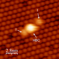 Molecular Dissociation on the SiC(0001) 3×3 Surface. In the framework of density functional theory, the adsorption of the halogenated polycyclic aromatic hydrocarbon 2,11-diiodohexabenzocoronene (HBC-I2) on the SiC(0001) 3×3 surface has been investigated. Nondissociative and dissociative molecular adsorption is considered, and simulated scanning tunneling microscopy (STM) images are compared with the corresponding experimental observations. Calculations show that dissociative adsorption is favorable and reveal the crucial importance of the extended flat carbon core on molecule—surface interactions in dissociative adsorption ; the iodine atom—surface interaction is of minor importance. Indeed, removing iodine atoms does not significantly affect the STM images of the central part of the molecule. This study shows that the dissociation of large halogenated polycyclic aromatic hydrocarbon molecules can occur on the SiC surface. This opens up interesting perspectives in the chemical reactivity and functionalization of wide band gap semiconductors. Molecular Dissociation on the SiC(0001) 3×3 Surface. In the framework of density functional theory, the adsorption of the halogenated polycyclic aromatic hydrocarbon 2,11-diiodohexabenzocoronene (HBC-I2) on the SiC(0001) 3×3 surface has been investigated. Nondissociative and dissociative molecular adsorption is considered, and simulated scanning tunneling microscopy (STM) images are compared with the corresponding experimental observations. Calculations show that dissociative adsorption is favorable and reveal the crucial importance of the extended flat carbon core on molecule—surface interactions in dissociative adsorption ; the iodine atom—surface interaction is of minor importance. Indeed, removing iodine atoms does not significantly affect the STM images of the central part of the molecule. This study shows that the dissociation of large halogenated polycyclic aromatic hydrocarbon molecules can occur on the SiC surface. This opens up interesting perspectives in the chemical reactivity and functionalization of wide band gap semiconductors. |
article : Ph. Sonnet, L. Stauffer, M. Gille, D. Bléger, S. Hecht, C. Cejas, G. Dujardin, A.J. Mayne, “Molecular dissociation on the SiC(0001)-3x3 surface”, Chem. Phys. Chem. 17, 3900 (2016)
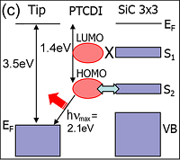 Single-molecule light emission at room temperature on a wide-band-gap semiconductor. Room-temperature light emission from single chemisorbed perylene based molecules adsorbed on silicon carbide (SiC) is probed by scanning tunneling microscopy (STM). A new approach to STM-induced luminescence of a single molecule is explored using a wide-band-gap semiconductor to decouple electronically the molecule from the surface. The maximum photon energy of the light emission from the molecule shows a fixed shift of 1.5 eV relative to the maximum energy of the tunnel electrons. This is consistent with the photons being generated by inelastic electron tunneling between the HOMO and the unoccupied electronic states of the STM tip. Single-molecule light emission at room temperature on a wide-band-gap semiconductor. Room-temperature light emission from single chemisorbed perylene based molecules adsorbed on silicon carbide (SiC) is probed by scanning tunneling microscopy (STM). A new approach to STM-induced luminescence of a single molecule is explored using a wide-band-gap semiconductor to decouple electronically the molecule from the surface. The maximum photon energy of the light emission from the molecule shows a fixed shift of 1.5 eV relative to the maximum energy of the tunnel electrons. This is consistent with the photons being generated by inelastic electron tunneling between the HOMO and the unoccupied electronic states of the STM tip. |
article : H. Yang, A.J. Mayne, G. Comtet, G. Dujardin, Y. Kuk, S. Nagarajan, A. Gourdon, “Single molecule luminescence induced by STM of chemisorbed PTCDI on silicon carbide”, Phys. Rev. B 90, 125427 (2014)
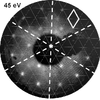
 STM imagery and density functional calculations of C60 fullerene adsorption on the 6H-SiC(0001)-3×3 surface. We show that chemisorption of individual C60 molecules occurs through the formation of one bond to one silicon adatom only in contrast to multiple bond formation on other semiconducting surfaces.We observe three stable adsorption sites with respect to the Si adatoms of the surface unit cell. Comprehensive DFT calculations give different adsorption energies for the three most abundant sites showing that van der Waals forces between the C60 molecule and the neighboring surface atoms need to be considered. The C60 molecules are observed to form small clusters even at low coverage indicating the presence of a mobile molecular precursor state and non negligible intermolecular interactions. STM imagery and density functional calculations of C60 fullerene adsorption on the 6H-SiC(0001)-3×3 surface. We show that chemisorption of individual C60 molecules occurs through the formation of one bond to one silicon adatom only in contrast to multiple bond formation on other semiconducting surfaces.We observe three stable adsorption sites with respect to the Si adatoms of the surface unit cell. Comprehensive DFT calculations give different adsorption energies for the three most abundant sites showing that van der Waals forces between the C60 molecule and the neighboring surface atoms need to be considered. The C60 molecules are observed to form small clusters even at low coverage indicating the presence of a mobile molecular precursor state and non negligible intermolecular interactions. |
Article : T. Ovramenko, F. Spillebout, F.C. Bocquet, A.J. Mayne, G. Dujardin, Ph. Sonnet, L. Stauffer, Y. Ksari, J.-M. Themlin, "STM imagery and DFT calculations of C60 fullerene adsorption on the SiC(0001)-3x3 surface", Phys. Rev. B 87, 155421 (2013)
 Influence of charge transfer doping on the morphologies of C60 islands on hydrogenated diamond C(100)-(2x1). The adsorption and island formation of C60 fullerenes on the hydrogenated C(100)-(2x1):H diamond
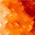
surface is studied using high-resolution noncontact atomic force microscopy in ultrahigh vacuum. At room temperature, C60 fullerene molecules assemble into monolayer islands, exhibiting a hexagonally close-packed internal structure. Dewetting is observed when raising the substrate temperature above approximately 505 K, resulting in two-layer high islands. In contrast to the monolayer islands, these double-layer islands form extended wetting layers. This peculiar behavior is explained by an increased molecule-substrate binding energy in the case of double-layer islands, which originates from charge transfer doping. Only upon further increasing the substrate temperature to approximately 615 K, the wetting layer desorbs, corresponding to a binding energy of the charge transfer-stabilized film of 1.7 eV. Influence of charge transfer doping on the morphologies of C60 islands on hydrogenated diamond C(100)-(2x1). The adsorption and island formation of C60 fullerenes on the hydrogenated C(100)-(2x1):H diamond
surface is studied using high-resolution noncontact atomic force microscopy in ultrahigh vacuum. At room temperature, C60 fullerene molecules assemble into monolayer islands, exhibiting a hexagonally close-packed internal structure. Dewetting is observed when raising the substrate temperature above approximately 505 K, resulting in two-layer high islands. In contrast to the monolayer islands, these double-layer islands form extended wetting layers. This peculiar behavior is explained by an increased molecule-substrate binding energy in the case of double-layer islands, which originates from charge transfer doping. Only upon further increasing the substrate temperature to approximately 615 K, the wetting layer desorbs, corresponding to a binding energy of the charge transfer-stabilized film of 1.7 eV. |
Article : M. Nimmrich, M. Kittelmann, P. Rahe, W. Harneit, A.J. Mayne, G. Dujardin, A. Kühnle, "Influence of charge transfer doping on the morphology of C60 islands on hydrogenated diamond C(100)-2x1", Phys. Rev. B 85, 035420 (2012)
 The paradox of an insulating contact between a chemisorbed molecule and a wide band gap semiconductor surface. Controlling the intrinsic optical and electronic properties of a single molecule adsorbed on a surface requires electronic decoupling of some molecular orbitals from the surface states. Using a combination of Scanning tunniling microscopy and DFT calculations, we find that the LUMO of the DHH-PTCDI molecule adsorbed on the SiC(0001)-3x3 surface molecule is invisible in I(V) spectra due to the absence of any surface or bulk states and that the HOMO has a very low saturation current in I(z) spectra. These results present a paradox that the molecular orbitals are electronically isolated from the surface of the wide band gap semiconductor even though strong chemical bonds are formed. The paradox of an insulating contact between a chemisorbed molecule and a wide band gap semiconductor surface. Controlling the intrinsic optical and electronic properties of a single molecule adsorbed on a surface requires electronic decoupling of some molecular orbitals from the surface states. Using a combination of Scanning tunniling microscopy and DFT calculations, we find that the LUMO of the DHH-PTCDI molecule adsorbed on the SiC(0001)-3x3 surface molecule is invisible in I(V) spectra due to the absence of any surface or bulk states and that the HOMO has a very low saturation current in I(z) spectra. These results present a paradox that the molecular orbitals are electronically isolated from the surface of the wide band gap semiconductor even though strong chemical bonds are formed. |
Article : H. Yang, O. Boudrioua, A.J. Mayne, G. Comtet, G. Dujardin, Ph. Sonnet, L. Stauffer, S. Nagarajan, A. Gourdon, Phys. Chem. Chem. Phys. 14, 1700 (2012)
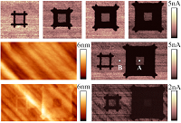 Low voltage fabrication of sub-nanometer insulating layers on hydrogenated diamond. A new regime of electrochemical anodic oxidation induced by an atomic force microscope (AFM) is demonstrated. With this approach, insulating nanostructures on a hydrogenated diamond surface can be produced. Low voltage fabrication of sub-nanometer insulating layers on hydrogenated diamond. A new regime of electrochemical anodic oxidation induced by an atomic force microscope (AFM) is demonstrated. With this approach, insulating nanostructures on a hydrogenated diamond surface can be produced. |
Article : T. Wang, E. Boer-Duchemin, E. Tranvouez, R. Cartwright, G. Comtet, G. Dujardin, A.J. Mayne, J. Appl. Phys. 110, 034311 (2011)