
Accueil > Équipes scientifiques > Surfaces, Interfaces, Molecules & 2D Materials (SIM2D) > New 2D Materials : Silicene, Phosphorene, Bismuthene
New 2D Materials : Silicene, Phosphorene, Bismuthene
Silicene forms a buckled honeycomb structure when grown on many surfaces as single layers or nanowires. The first experimental observations (APL 2010, 97, 223109) confirmed the initial theoretical proposals. Self-assembled silicene nanoribbons and silicene sheets deposited on different crystalline surfaces are studied with STM.
Techniques : RT STM - LT STM - SXRD - ALE - AES - LEED - Synchrotron
New 2D Materials : Silicene, Phosphorene, …
Silicene
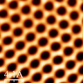
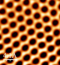
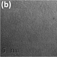
Leader : Hamid Oughaddou Participants : Hanna Enriquez, Andrew Mayne & Gérald Dujardin Students : Xiao Zhang, Khalid Quertite & Wei Zhang Silicene is a honeycomb structure of silicon which grows as single layers or nanowires on silver surfaces. Although theorists had speculated about the existence and possible properties of silicene, the first experimental observations were reported by B. Lalmi, H. Oughaddou, H. Enriquez, et al. in 2010. Using the STM, self-assembled silicene nanoribbons and silicene sheets deposited on a silver crystal are studied with atomic resolution. The honeycomb structure observed in the STM images is reminiscent of the honeycomb structure of graphene. Density Functional Theory calculations show that silicon atoms form stable honeycomb but buckled structures on silver. |
Techniques : RT STM - LT STM - Surface X-Ray Diffraction (SXRD) - ALE - Auger Electron Spectroscopy (AES) - LEED - Synchrotron Radiation
Highlights
|
Article : E. Neziri, W. Zhang, A. Smogunov, A. J. Mayne, A. Kara, Y. J. Dappe, H. Oughaddou, "Structural and Electronic Properties of Bi/Au(110)", Nanotechnology 34, 235601 (2023)
 First steps of silicene growth on an insulating thin-film : effect of the substrate temperature. Silicene is a two-dimensional (2D) material with very promising electronic properties for applications in silicon modern technology. However, the first experimental synthesis of silicene on metallic surfaces shows strong interactions between the silicene and its substrate, which can alter its electronic properties. Here, we report on the first steps of silicene growth on an insulating surface (NaCl) using scanning tunneling microscopy (STM), low energy electron diffraction (LEED), Auger electron spectroscopy (AES), and angle-resolved photoemission spectroscopy (ARPES). We demonstrate the importance of temperature annealing in the growth of silicene on NaCl. Indeed, after deposition of silicon on the NaCl/Ag(110) surface, we observe the following stages : (i) at room temperature, the silicon atoms accumulate on top of the NaCl layer without any given order. (ii) At 60 °C, silicon dimers start to grow on the NaCl. (iii) At 140 °C, these dimers form a 2D silicon chains on the surface. (iv) After a post-annealing at 200 °C, evident 2D silicon nanoribbons with a honeycomb-like structure were observed. Our results of the first silicene growth stages on an insulating surface are a necessary step for exploring its growth mechanism further. First steps of silicene growth on an insulating thin-film : effect of the substrate temperature. Silicene is a two-dimensional (2D) material with very promising electronic properties for applications in silicon modern technology. However, the first experimental synthesis of silicene on metallic surfaces shows strong interactions between the silicene and its substrate, which can alter its electronic properties. Here, we report on the first steps of silicene growth on an insulating surface (NaCl) using scanning tunneling microscopy (STM), low energy electron diffraction (LEED), Auger electron spectroscopy (AES), and angle-resolved photoemission spectroscopy (ARPES). We demonstrate the importance of temperature annealing in the growth of silicene on NaCl. Indeed, after deposition of silicon on the NaCl/Ag(110) surface, we observe the following stages : (i) at room temperature, the silicon atoms accumulate on top of the NaCl layer without any given order. (ii) At 60 °C, silicon dimers start to grow on the NaCl. (iii) At 140 °C, these dimers form a 2D silicon chains on the surface. (iv) After a post-annealing at 200 °C, evident 2D silicon nanoribbons with a honeycomb-like structure were observed. Our results of the first silicene growth stages on an insulating surface are a necessary step for exploring its growth mechanism further.
|
Article : K. Quertite, H. Enriquez, N. Trcera, P. Lagarde, A. Bendounan, A. J. Mayne, G. Dujardin, A. El Kenz, A. Benyoussef, A. Kara, H. Oughaddou, "First steps of silicene growth on an insulating thin-film : effectof the substrate temperature", Eur. Phys. J. Appl. Phys. 98, 41 (2023)
 Flat epitaxial quasi-1D phosphorene chains. The emergence of peculiar phenomena in 1D phosphorene chains (P chains) has been proposed in theoretical studies, notably the Stark and Seebeck effects, room temperature magnetism, and topological phase transitions. Attempts so far to fabricate P chains, using the top-down approach starting from a few layers of bulk black phosphorus, have failed to produce reliably precise control of P chains. We show that molecular beam epitaxy gives a controllable bottom-up approach to grow atomically thin, crystalline 1D flat P chains on a Ag (111) substrate. Scanning tunneling microscopy, angle-resolved photoemission spectroscopy, and density functional theory calculations reveal that the armchair-shaped chains are semiconducting with an intrinsic 1.80 ± 0.20 eV band gap. This could make these P chains an ideal material for opto-electronic devices. Flat epitaxial quasi-1D phosphorene chains. The emergence of peculiar phenomena in 1D phosphorene chains (P chains) has been proposed in theoretical studies, notably the Stark and Seebeck effects, room temperature magnetism, and topological phase transitions. Attempts so far to fabricate P chains, using the top-down approach starting from a few layers of bulk black phosphorus, have failed to produce reliably precise control of P chains. We show that molecular beam epitaxy gives a controllable bottom-up approach to grow atomically thin, crystalline 1D flat P chains on a Ag (111) substrate. Scanning tunneling microscopy, angle-resolved photoemission spectroscopy, and density functional theory calculations reveal that the armchair-shaped chains are semiconducting with an intrinsic 1.80 ± 0.20 eV band gap. This could make these P chains an ideal material for opto-electronic devices.
|
Article : W. Zhang, H. Enriquez, Y.-F. Tong, A. J. Mayne, A. Bendounan, A. Smogunov, Y. J. Dappe, A. Kara, G. Dujardin, H. Oughaddou, "Flat epitaxial quasi-1D phosphorene chains", Nature Communications 12, 5160 (2021) Open Access INP
 Phase transition from Au–Te surface alloy towards tellurene-like monolayer. Two-dimensional (2D) chalcogen-based layers will be among the next generation of materials for potential high-tech applications. We present the structural and electronic properties of Tellurium (Te) deposited on the Au(111) surface by high temperature vapor deposition in UHV. We discuss the possible scenarios for the formation of 2D layers ; either AuTe2 metal dichalcogenide, or Au–Te alloy or a single Tellurene layer. Low energy electron diffraction (LEED) and scanning tunneling microscopy (STM) show the existence of several surface reconstructions depending on the Te film thickness in the sub-monolayer regime. We observe the survival of the well-known spin-split Shockley state of the Au(111) surface after Te deposition. The state is shifted to higher binding energy, suggesting a charge transfer at the interface. For 0.33 ML Te, new dispersive bands in the angle-resolved photoemission (ARPES), are due to the strong hybridization between the electronic states of Te and Au. The low intensity and back-folding at the boundaries of the reduced surface Brillouin zone (R-SBZ), prove that these electronic bands represent a naturel 2D electron gas, strongly disturbed by the surface reconstruction. This indicates the fromation of a surface Au–Te alloy. At 0.5 ML Te, a rich, thickness-dependent transition develops from the surface alloy to Tellurene-like structure which excludes the growth of AuTe2 monolayer. Both the surface alloy and the Tellurene monolayer are semiconducting with an occupied-state gap of 0.65 eV. Phase transition from Au–Te surface alloy towards tellurene-like monolayer. Two-dimensional (2D) chalcogen-based layers will be among the next generation of materials for potential high-tech applications. We present the structural and electronic properties of Tellurium (Te) deposited on the Au(111) surface by high temperature vapor deposition in UHV. We discuss the possible scenarios for the formation of 2D layers ; either AuTe2 metal dichalcogenide, or Au–Te alloy or a single Tellurene layer. Low energy electron diffraction (LEED) and scanning tunneling microscopy (STM) show the existence of several surface reconstructions depending on the Te film thickness in the sub-monolayer regime. We observe the survival of the well-known spin-split Shockley state of the Au(111) surface after Te deposition. The state is shifted to higher binding energy, suggesting a charge transfer at the interface. For 0.33 ML Te, new dispersive bands in the angle-resolved photoemission (ARPES), are due to the strong hybridization between the electronic states of Te and Au. The low intensity and back-folding at the boundaries of the reduced surface Brillouin zone (R-SBZ), prove that these electronic bands represent a naturel 2D electron gas, strongly disturbed by the surface reconstruction. This indicates the fromation of a surface Au–Te alloy. At 0.5 ML Te, a rich, thickness-dependent transition develops from the surface alloy to Tellurene-like structure which excludes the growth of AuTe2 monolayer. Both the surface alloy and the Tellurene monolayer are semiconducting with an occupied-state gap of 0.65 eV.
|
Article : M. Bouaziz, W. Zhang, Y.-F. Tong, H. Oughaddou, H. Enriquez, R. Mlika, H. Korri-Youssoufi, Z. Chen, H. Xiong, Y. Cheng, A. Bendounan, "Phase transition from Au–Te surface alloy towards tellurene-like monolayer", 2D Materials 8, 015029 (2021)
 Silicene Nanoribbons on an Insulating Thin Film. Silicene, a new 2D material has attracted intense research because of the ubiquitous use of silicon in modern technology. However, producing freestanding silicene has proved to be a huge challenge. Until now, silicene could be synthesized only on metal surfaces where it naturally forms strong interactions with the metal substrate that modify its electronic properties. Here, the authors report the first experimental evidence of silicene sheet on an insulating NaCl thin film. This work represents a major breakthrough, for the study of the intrinsic properties of silicene, and by extension to other 2D materials that have so far only been grown on metal surfaces. Silicene Nanoribbons on an Insulating Thin Film. Silicene, a new 2D material has attracted intense research because of the ubiquitous use of silicon in modern technology. However, producing freestanding silicene has proved to be a huge challenge. Until now, silicene could be synthesized only on metal surfaces where it naturally forms strong interactions with the metal substrate that modify its electronic properties. Here, the authors report the first experimental evidence of silicene sheet on an insulating NaCl thin film. This work represents a major breakthrough, for the study of the intrinsic properties of silicene, and by extension to other 2D materials that have so far only been grown on metal surfaces.
|
Article : K. Quertite, H. Enriquez, N. Trcera, Y. Tong, A. Bendounan, A. J. Mayne, G. Dujardin, P. Lagarde, A. El Kenz, A. Benyoussef, Y. J. Dappe, A. Kara, H. Oughaddou, "Silicene Nanoribbons on an Insulating Thin Film", Advanced Functional Materials 31, 2007013 (2021)
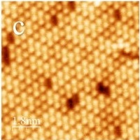
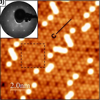
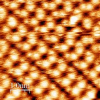
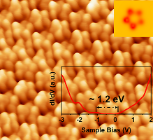 Phosphorus Pentamers : Floating Nanoflowers. An experimental investigation of a new polymorphic 2D single layer of phosphorus on Ag(111) is presented. The atomically-resolved scanning tunneling microscopy images show a new 2D material composed of freely-floating phosphorus pentamers organized into a 2D layer, where the pentamers are aligned in close-packed rows. The scanning tunneling spectroscopy measurements reveal a semiconducting character with a band gap of 1.20 eV. This work presents the formation at low temperature of a new polymorphic 2D phosphorus layer composed of a floating 2D pentamer structure. The smooth curved terrace edges and a lack of any clear crystallographic orientation with respect to the Ag(111) substrate at room temperature indicates a smooth potential energy surface that is reminiscent of a liquid-like growth phase. This is confirmed by density functional theory calculations that find a small energy barrier of only 0.17 eV to surface diffusion of the pentamers (see Supporting Information). The formation of extended, homogeneous domains is a key ingredient to opening a new avenue to integrate this new 2D material into electronic devices. Phosphorus Pentamers : Floating Nanoflowers. An experimental investigation of a new polymorphic 2D single layer of phosphorus on Ag(111) is presented. The atomically-resolved scanning tunneling microscopy images show a new 2D material composed of freely-floating phosphorus pentamers organized into a 2D layer, where the pentamers are aligned in close-packed rows. The scanning tunneling spectroscopy measurements reveal a semiconducting character with a band gap of 1.20 eV. This work presents the formation at low temperature of a new polymorphic 2D phosphorus layer composed of a floating 2D pentamer structure. The smooth curved terrace edges and a lack of any clear crystallographic orientation with respect to the Ag(111) substrate at room temperature indicates a smooth potential energy surface that is reminiscent of a liquid-like growth phase. This is confirmed by density functional theory calculations that find a small energy barrier of only 0.17 eV to surface diffusion of the pentamers (see Supporting Information). The formation of extended, homogeneous domains is a key ingredient to opening a new avenue to integrate this new 2D material into electronic devices.
|
Article : W. Zhang, H. Enriquez, Y. Tong, A. J. Mayne, A. Bendounan, Y. J. Dappe, A. Kara, G. Dujardin, H. Oughaddou, "Phosphorus Pentamers : Floating Nanoflowers form a 2D network", Advanced Functional Materials 30, 2004531 (2020)
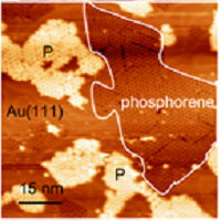 Blue phosphorene reactivity on Au(111). The synthesis of blue phosphorene by molecular beam epitaxy (MBE) has recently come under the spotlight due to its potential applications in electronic and optoelectronic devices. However, this synthesis remains a significant challenge. The surface reactivity between the P atoms and the Au atoms should be considered for the P/Au(111) system. In the MBE process, the temperature of the substrate is a key parameter for the growth of blue phosphorene. During the initial growth stage, irregularly shaped Phosphorus clusters grow on top of Au(111) surface at room temperature. When the substrate temperature is increased, these clusters transform into a phosphorene-like structure with a honeycomb lattice. An atom exchange reaction is observed between the P and first layer Au atoms under thermal activation at higher temperature, where the P atoms replace Au atoms to form a blue phosphorene structure within the top Au layer and at the step edges. Blue phosphorene reactivity on Au(111). The synthesis of blue phosphorene by molecular beam epitaxy (MBE) has recently come under the spotlight due to its potential applications in electronic and optoelectronic devices. However, this synthesis remains a significant challenge. The surface reactivity between the P atoms and the Au atoms should be considered for the P/Au(111) system. In the MBE process, the temperature of the substrate is a key parameter for the growth of blue phosphorene. During the initial growth stage, irregularly shaped Phosphorus clusters grow on top of Au(111) surface at room temperature. When the substrate temperature is increased, these clusters transform into a phosphorene-like structure with a honeycomb lattice. An atom exchange reaction is observed between the P and first layer Au atoms under thermal activation at higher temperature, where the P atoms replace Au atoms to form a blue phosphorene structure within the top Au layer and at the step edges.
|
Article : W. Zhang, H. Enriquez, X. Zhang, A. J. Mayne, A. Bendounan, Y. J. Dappe, A. Kara, G. Dujardin, H. Oughaddou, "Phosphorene Reactivity on the Au(111) surface", Nanotechnology 31, 495602 (2020)
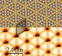
 Evidence of new 2D material : Cu2Te. Here, we report on the formation and characterization of an uncharted 2D material : ‘Cu2Te alloy monolayer on Cu(111) surface’. We have successfully grown a 2D binary Te-Cu alloy using a straightforward approach based on chemical deposition method. LEED and STM results reveal the existence of a well-ordered alloy monolayer characterized by (√3 × √3)R30◦ superstructure, while the XPS measurements indicate the presence of single chemical environment of the Te atoms associated with the Te-Cu bonding. Analysis of the valence band properties by ARPES ; in particular the electronic states close to the Fermi level suggests a strong hybridization between Te and Cu electronic states leading to an appearance of new dispersive bands localized at the surface alloy, which is confirmed by first-principles calculations. These bands are strongly influenced by the surface reconstruction and undergo a back-folding at the boundaries of the reduced surface Brillouin zone (SBZ). More interesting, a band gap of about 0.91 eV and a Rashba splitting in the conduction band are obtained. Evidence of new 2D material : Cu2Te. Here, we report on the formation and characterization of an uncharted 2D material : ‘Cu2Te alloy monolayer on Cu(111) surface’. We have successfully grown a 2D binary Te-Cu alloy using a straightforward approach based on chemical deposition method. LEED and STM results reveal the existence of a well-ordered alloy monolayer characterized by (√3 × √3)R30◦ superstructure, while the XPS measurements indicate the presence of single chemical environment of the Te atoms associated with the Te-Cu bonding. Analysis of the valence band properties by ARPES ; in particular the electronic states close to the Fermi level suggests a strong hybridization between Te and Cu electronic states leading to an appearance of new dispersive bands localized at the surface alloy, which is confirmed by first-principles calculations. These bands are strongly influenced by the surface reconstruction and undergo a back-folding at the boundaries of the reduced surface Brillouin zone (SBZ). More interesting, a band gap of about 0.91 eV and a Rashba splitting in the conduction band are obtained. |
Article : Y. Tong, M. Bouaziz, W. Zhang, B. Obeid, A. Loncle, H. Oughaddou, H. Enriquez, K. Chaouchi, V. Esaulov, Z. Chen, H. Xiong, Y. Cheng, A. Bendounan, "Evidence of new 2D material : Cu2Te", 2D Materials 7, 035010 (2020)
 Tip-induced oxidation of silicene nano-ribbons. We report on the oxidation of self-assembled silicene nanoribbons grown on the Ag (110) surface using scanning tunneling microscopy and high-resolution photoemission spectroscopy. The results show that silicene nanoribbons present a strong resistance towards oxidation using molecular oxygen. This can be overcome by increasing the electric field in the STM tunnel junction above a threshold of +2.6 V to induce oxygen dissociation and reaction. The higher reactivity of the silicene nanoribbons towards atomic oxygen is observed as expected. The HR-PES confirm these observations : even at high exposures of molecular oxygen, the Si 2p core-level peaks corresponding to pristine silicene remain dominant, reflecting a very low reactivity to molecular oxygen. Complete oxidation is obtained following exposure to high doses of atomic oxygen ; the Si 2p core level peak corresponding to pristine silicene disappears. Tip-induced oxidation of silicene nano-ribbons. We report on the oxidation of self-assembled silicene nanoribbons grown on the Ag (110) surface using scanning tunneling microscopy and high-resolution photoemission spectroscopy. The results show that silicene nanoribbons present a strong resistance towards oxidation using molecular oxygen. This can be overcome by increasing the electric field in the STM tunnel junction above a threshold of +2.6 V to induce oxygen dissociation and reaction. The higher reactivity of the silicene nanoribbons towards atomic oxygen is observed as expected. The HR-PES confirm these observations : even at high exposures of molecular oxygen, the Si 2p core-level peaks corresponding to pristine silicene remain dominant, reflecting a very low reactivity to molecular oxygen. Complete oxidation is obtained following exposure to high doses of atomic oxygen ; the Si 2p core level peak corresponding to pristine silicene disappears. |
Article : M. R. Tchalala, H. Enriquez, A. Bendounan, A. J. Mayne, G. Dujardin, A. Kara, H. Oughaddou, "Tip-induced oxidation of silicene nano-ribbons", Nanoscale Advances 2, 2309-2314 (2020)
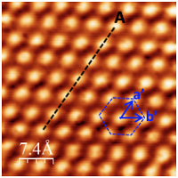
 Blue phosphorene. Phosphorene is a new 2D material composed of a single or few atomic layers of black phosphorus. Phosphorene has both an intrinsic tunable direct bandgap and high carrier mobility values, which make it suitable for a large variety of optical and electronic devices. However, the synthesis of single-layer phosphorene is a major challenge. The standard procedure to obtain phosphorene is by exfoliation. More recently, the epitaxial growth of single-layer phosphorene on Au(111) was investigated by molecular beam epitaxy and the obtained structure described as a blue phosphorene sheet. In the present study, large areas of high-quality monolayer phosphorene, with a bandgap value equal to at least 0.8 eV, are synthesized on Au(111). The experimental investigations, coupled with density functional theory calculations, give evidence of two distinct phases of blue phosphorene on Au(111), instead of one as previously reported, and their atomic structures are determined. Blue phosphorene. Phosphorene is a new 2D material composed of a single or few atomic layers of black phosphorus. Phosphorene has both an intrinsic tunable direct bandgap and high carrier mobility values, which make it suitable for a large variety of optical and electronic devices. However, the synthesis of single-layer phosphorene is a major challenge. The standard procedure to obtain phosphorene is by exfoliation. More recently, the epitaxial growth of single-layer phosphorene on Au(111) was investigated by molecular beam epitaxy and the obtained structure described as a blue phosphorene sheet. In the present study, large areas of high-quality monolayer phosphorene, with a bandgap value equal to at least 0.8 eV, are synthesized on Au(111). The experimental investigations, coupled with density functional theory calculations, give evidence of two distinct phases of blue phosphorene on Au(111), instead of one as previously reported, and their atomic structures are determined. |
Article : W. Zhang, H. Enriquez, Y.F. Tong, A. Bendounan, A. Kara, A.P. Seitsonen, A.J. Mayne, G. Dujardin, H. Oughaddou, "Epitaxial Synthesis of Blue Phosphorene", Small 14, 1804066 (2018)
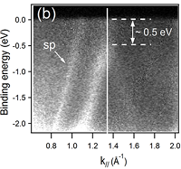
Dirac cone in 2D silicene. The remarkable properties of graphene stem from its two-dimensional (2D) structure, with a linear dispersion of the electronic states at the corners of the Brillouin zone (BZ) forming a Dirac cone. Since then, other 2D materials have been suggested based on boron, silicon, germanium, phosphorus, tin, and metal di-chalcogenides. Here, we present an experimental investigation of a single silicon layer on Au(111) using low energy electron diffraction (LEED), high resolution angle-resolved photoemission spectroscopy (HR-ARPES), and scanning tunneling microscopy (STM). The HR-ARPES data show compelling evidence that the silicon based 2D overlayer is responsible for the observed linear dispersed feature in the valence band, with a Fermi velocity of vF = 10+6 m.s−1 comparable to that of graphene. The STM images show extended and homogeneous domains, offering a viable route to the fabrication of silicene-based opto-electronic devices. |
Article : S. Sadeddine, H. Enriquez, A. Bendounan, P.K. Das, I. Vobornik, A.J. Mayne, G. Dujardin, F. Sirotti, A. Kara, H. Oughaddou, “Compelling experimental evidence of a Dirac cone in the electronic structure of a 2D Silicon layer”, Scientific Reports 7, 44400 (2017)
Silicene : A promising new 2D material. Silicene is emerging as a two-dimensional material with very attractive electronic properties for a wide range of applications ; it is a particularly promising material for nano-electronics in silicon-based technology. Over the last decade, the existence and stability of silicene has been the subject of much debate. Theoretical studies of free-standing silicene predicted a puckered honeycomb structure with electronic properties resembling those of graphene. However, experimental fabrication of silicene has been achieved only through epitaxial growth on crystalline surfaces. Since the first experimental evidence of the formation of silicene on Ag(110) and Ag(111) in 2010, this very active field has developed with the recent growth of silicene on Ir(111), ZrB2(0001) and Au(110) substrates. In this review, we discuss the experimental and theoretical studies of silicene performed to date. Special attention is given to different experimental studies of the electronic properties of silicene on metal substrates. New avenues for the growth of silicene on other substrates with different chemical characteristics are presented along with foreseeable applications such as nano-devices and novel batteries. |
Review : H. Oughaddou, H. Enriquez, M.R. Tchalala, H. Yildirim, A.J. Mayne, A. Bendounan, G. Dujardin, M. Ait Ali, A. Kara, “Silicene : A promising new 2D material”, Prog. Surf. Science 90, 46-83 (2015)
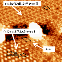
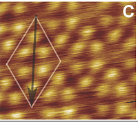
Atomic and electronic structures of the (√13x√13)R13.9° of silicene sheet on Ag(111). Using scanning tunneling microscopy, low energy electron diffraction measurements, and ab initio calculations based on density functional theory, we present atomic models of the (√13×√13)R13.9◦ silicene superstructure grown on Ag(111). The STM images reveal two co-existing atomic arrangements with two different orientations of the silicene sheet relative to the Ag(111) surface. DFT calculations with and without the inclusion of van der Waals interactions show corrugated Si atomic positions for both orientations implying a significant interaction with Ag(111) surface. The electronic structure of both silicene and Ag(111) surface are sufficiently affected that new interface states emerge close to the Fermi level. |
Article : M. R. Tchalala, H. Enriquez, H. Yildirim, A. Kara, A. Mayne, G. Dujardin, M. Ait Ali and H. Oughaddou, "Atomic and electronic structures of the (√13x√13)R13.9° of silicene sheet on Ag(111)", Appl. Surf. Sci. 303, 61–66 (2014)
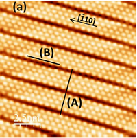
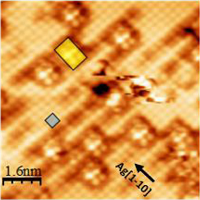
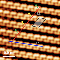
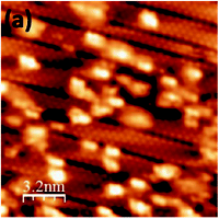
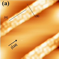
Atomic structure of silicene nanoribbons on Ag(110). The growth of silicene nano-ribbons (NRs) on Ag(110) substrate is re-investigated using scanning tunneling microscopy (STM) and low energy electron diffraction (LEED). Deposition of one silicon monolayer at 230°C induces the formation of one-dimensional 1.6 nm wide silicene nanoribbons into a well-ordered compact array with a nanometer-scale pitch of just 2 nm. Based on the STM analysis we derived an atomic model of the silicene nanoribbons (NRs) where they are substantially buckled, and quantum confinement of the electrons in the NRs contribute to electronic density of states. |
article : M. R. Tchalala, H. Enriquez, A. Mayne, A. Kara, G. Dujardin, M. Ait Ali and H. Oughaddou, "Atomic structure of silicene nanoribbons on Ag(110)", Journal of Physics : Conference Series 491, 012002 (2014)
Silicon Sheets by Redox Assisted Chemical Exfoliation. In this paper, we report the direct chemical synthesis of silicon sheets in gram-scale quantities by chemical exfoliation of pre-processed calcium disilicide (CaSi2). We have used a combination of x-ray photoelectron spectroscopy, transmission electron microscopy and energy-dispersive x-ray spectroscopy to characterize the obtained silicon sheets. We found that the clean and crystalline silicon sheets show a two-dimensional hexagonal graphitic structure. |
article : M.R. Tchalala, M. Ait Ali, H. Enriquez, A. Kara, A. Lachgar, S. Yagoubi, E. Foy, E. Vega, A. Bendounan, M. Silly, F. Sirroti, S. Nitshe, D. Chaudanson, H. Jamgotchian, B. Aufray, A.J. Mayne, G. Dujardin, H. Oughaddou, “Silicon Sheets by Redox Assisted Chemical Exfoliation”, J. Phys. Condens. Mat. 25, 442001 (2013)
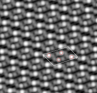
First NC-AFM images of silicene. We present the first non-contact atomic force microscopy (nc-AFM) of a silicene on a silver (Ag) surface, obtained by combining non-contact atomic force microscopy and scanning tunneling microscopy (STM). STM images over large areas of silicene grown on the Ag(111) surface show both (root13 x root13)R13.9 and (4 x 4) superstructures. For the widely observed (4 x 4) structure, the observed nc-AFM image is very similar to the one recorded by STM. The structure resolved by nc-AFM is compatible with only one out of two silicon atoms being visible. This indicates unambiguously a strong buckling of the silicene honeycomb layer. |
Article : Z. Majzik, M. R. Tchalala, M. Švec, P. Hapala, H. Enriquez, A. Kara, A.J. Mayne, G. Dujardin, P. Jelínek, H. Oughaddou, "Combined AFM and STM measurements of a silicene sheet grown on the Ag(111) surface", J. Phys. Condens. Mat. 25, 225301 (2013)
Formation of one-dimensional self-assembled silicon nanoribbons on Au(110)-(2x1). We report results on the self-assembly of silicon nanoribbons (NRs) on the (2x1) reconstructed Au(110) surface under ultra-high vacuum conditions. Upon adsorption of 0.2 monolayer (ML) of silicon the (2x1), reconstruction of Au(110) is replaced by an ordered surface alloy. Above this coverage, a new superstructure is revealed by low energy electron diffraction (LEED), which becomes sharper at 0.3 Si ML. This superstructure corresponds to Si nanoribbons all oriented along the (110) direction as revealed by LEED and scanning tunneling microscopy (STM). STM and high- resolution photoemission spectroscopy indicate that the nanoribbons are flat and predominantly 1.6 nm wide. In addition, the silicon atoms show signatures of two chemical environments corresponding to the edge and center of the ribbons. |
Article : M.R. Tchalala, H. Enriquez, A.J. Mayne, A. Kara, S. Roth, M.G. Silly, A. Bendounan, F. Sirroti, Th. Greber, B. Aufray, G. Dujardin, H. Oughaddou, "Formation of one-dimensional self-assembled silicon nanoribbons on Au(110)-2x1", Appl. Phys. Lett. 102, 083107 (2013)
Adsorption of silicon on Au(110) : an ordered 2D surface alloy. We show experimental evidence for the formation of a two dimensional Si/Au(110) surface alloy. In this study, we have used a combination of scanning tunneling microscopy, low energy electron diffraction, Auger electron spectroscopy, and ab initio calculations based on density functional theory. A highly ordered and stable Si-Au surface alloy is observed subsequent to growth of a sub-monolayer of silicon on an Au(110) substrate kept above the eutectic temperature. |
Article : H. Enriquez, A.J. Mayne, A. Kara, S. Vizzini, S. Roth, B. Lalmi, A.P. Seitsonen, B. Aufray, Th. Greber, R. Belkhou, G. Dujardin, H. Oughaddou Appl. Phys. Lett. 101, 021605 (2012)