
Accueil > Équipes scientifiques > Surfaces, Interfaces, Molecules & 2D Materials (SIM2D) > Graphène : molécules et transport > Graphene : Molecules & Transport
Graphene : Molecules & Transport
Graphene
Leader : Andrew Mayne Participants : Hamid Oughaddou, Hanna Enriquez, Philippe Roncin, Gérald Dujardin Student : Nian Jheng Wu Past Contributors : Mali Zhao, Laury Martins-Lopès, Heejun Yang & Geneviève Comtet STM topography and I(V), I(Z) and Z(V) spectroscopies are used to study the atomic-scale structural, electronic and electron transport properties of graphene epitaxially grown on SiC substrates. STM is also used to investigate self-assembling and reactivity of molecules on graphene with the aim to locally modify the electronic properties of graphene. |
Techniques : Room temperature STM - STS, UHV, molecular deposition
Highlights
|
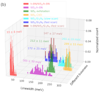
article : F. Shao, S. Y. Woo, N. J. Wu, R. Schneider, A. J. Mayne, S. Michaelis de Vasconcellos, A. Arora, B. J. Carey, J. A. Preuß, N. Bonnet, M. Och, C. Mattevi, K. Watanabe, T. Taniguchi, Z. Niu, R. Bratschitsch, and L. H. G. Tizei, “Substrate influence on transition metal dichalcogenide monolayer exciton absorption linewidth broadening” Physical Review Materials 6, 074005 (2022)
 Detection of graphene’s divergent orbital diamagnetism at the Dirac point. The electronic properties of graphene have been intensively investigated over the past decade. However, the singular orbital magnetism of undoped graphene, a fundamental signature of the characteristic Berry phase of graphene’s electronic wave functions, has been challenging to measure in a single flake. Using a highly sensitive giant magnetoresistance (GMR) sensor, we have measured the gate voltage–dependent magnetization of a single graphene monolayer encapsulated between boron nitride crystals. The signal exhibits a diamagnetic peak at the Dirac point whose magnetic field and temperature dependences agree with long-standing theoretical predictions. Our measurements offer a means to monitor Berry phase singularities and explore correlated states generated by the combined effects of Coulomb interactions, strain, or moiré potentials.
article : J. Vallejo Bustamante, N.-J. Wu , C. Fermon, M. Pannetier-Lecoeur, T. Wakamura, K. Watanabe, T. Taniguchi, T. Pellegrin, A. Bernard, S. Daddinounou, V. Bouchiat, S. Guéron, M. Ferrier, G. Montambaux, and H. Bouchiat, “Detection of graphene’s divergent orbital diamagnetism at the Dirac point” Science 374, 1399-1402 (2021)
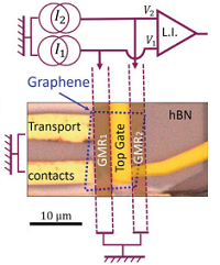
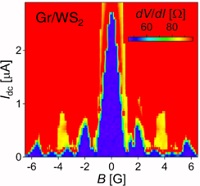 Spin-Orbit-Enhanced Robustness of Supercurrent in Graphene/WS2 Josephson Junctions. We demonstrate the enhanced robustness of the supercurrent through graphene-based Josephson junctions in which strong spin-orbit interactions (SOIs) are induced. We compare the persistence of a supercurrent at high out-of-plane magnetic fields between Josephson junctions with graphene on hexagonal boron-nitride and graphene on WS2, where strong SOIs are induced via the proximity effect. We find that in the shortest junctions both systems display signatures of induced superconductivity, characterized by a suppressed differential resistance at a low current, in magnetic fields up to 1 T. In longer junctions, however, only graphene on WS2 exhibits induced superconductivity features in such high magnetic fields, and they even persist up to 7 T. We argue that these robust superconducting signatures arise from quasiballistic edge states stabilized by the strong SOIs induced in graphene by WS2.
article : T. Wakamura, N.-J. Wu , A. D. Chepelianskii, S. Guéron, M. Och, M. Ferrier, T. Taniguchi, K. Watanabe, C. Mattevi, and H. Bouchiat, “Spin-Orbit-Enhanced Robustness of Supercurrent in Graphene/WS2 Josephson Junctions” Phys. Rev. Lett. 125, 266801 (2020)
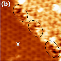
 Sub-molecular spectroscopy and temporary molecular charging of Ni-Phthalocyanine on graphene by STM. In this study, the self-assembled molecular network and electronic properties of Ni-phthalocyanine (NiPc) molecules on monolayer graphene (MLG)/6H-SiC(0001) were studied by room temperature Scanning Tunnelling Microscopy (STM) and Density Functional Theory (DFT) calculations. In this study, a very weak electronic coupling between the graphene and the NiPc molecules is found. This is due to the very small charge transfer of only 0.035e- per molecule. The weak molecule–graphene interaction has two observable consequences : sub-molecular resolution was obtained in the STM spectroscopy at room-temperature with the molecules adsorbed directly on the graphene, and the occupied and unoccupied molecular resonance peaks were observed to shift their position in energy as a function of the tip–surface distance. This is due to the temporary local charging (either positive or negative) that is achieved by decreasing the surface voltage under the STM tip. This may have important consequences for future studies of the opto-electronic properties of such hybrid graphene–molecule systems.
article : M. Zhao, F. Al Marzouqi, E. Duverger, Ph. Sonnet, G. Dujardin, A.J. Mayne, “Sub-molecular spectroscopy and temporary molecular charging of Ni-Phthalocyanine on graphene by STM” Phys. Chem. Chem. Phys. 20, 19507 (2018)
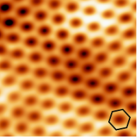
 Helium diffraction on SiC grown graphene, qualitative and quantitative description with the hard corrugated wall model. Monolayer epitaxial graphene grown on 6H-SiC(0001) was recently investigated by grazing-incidence fastatom diffraction and analyzed with an ab initio electronic density calculation and with exact atomic diffraction methods. With these results as a reference, the hard-corrugated-wall model (HCW) is used as a complementary analytic approach to link binary potentials to the observed atomic corrugation. The main result is that the HCW model reproduces the macroscopic corrugation of the moiré pattern on a quantitative level, suggesting that soft-wall corrections may be neglected for macroscopic superstructures, allowing straightforward analysis in terms of a one-dimensional corrugation function.
 |
article : M. Debiossac, A. Zugarramurdi, Z. Mu, P. Lunca-Popa, A.J. Mayne, P. Roncin, "Helium diffraction on SiC grown graphene, qualitative and quantitative description with the hard corrugated wall model”, Phys. Rev. B 94, 205403 (2016)
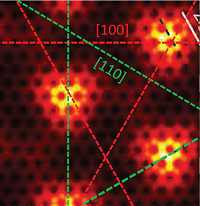
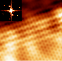
 Measuring the flatness of graphene with fast atoms. We present a grazing incidence fast atom diffraction (GIFAD) study of monolayer graphene on 6H-SiC(0001). This system shows a Moiré-like 13x13 superlattice above the reconstructed carbon buffer layer. The averaging property of GIFAD results in electronic and geometric corrugations that are well decoupled ; the graphene honeycomb corrugation is only observed with the incident beam parallel to the zigzag direction while the geometric corrugation arising from the superlattice is revealed along the armchair direction. Full-quantum calculations of the diffraction patterns show the very high GIFAD sensitivity to the amplitude of the surface corrugation. The best agreement between the calculated and measured diffraction intensities yields a corrugation height of 0.27A +- 0.03A .
 |
article : A. Zugarramurdi, M. Debiossac, P. Lunca-Popa, A. J. Mayne, A. Momeni, A. G. Borisov, Z. Mu, P. Roncin, H. Khemliche, "Determination of the geometric corrugation of graphene on SiC(0001) by grazing incidence fast atom diffraction", Appl. Phys. Lett. 106, 101902 (2015)
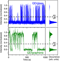
Fluorescence Lifetime and Blinking of Individual Semiconductor Nanocrystals on Graphene. A new class of optoelectronic nanodevices consisting of 0D semiconductor nanocrystals and 2D single graphene layers may be used to investigate and control the transfer of energy and charge in low-dimensional systems. The fluorescence dynamics of individual colloidal quantum dots (QDs) on graphene are investigated on both the nanosecond time scale (fluorescence lifetime) and the 1−100 s time scale (blinking statistics). We find that (i) a nonradiative energy transfer rate of ≈5 × 10+8 s−1 from the reduced lifetimes of QDs on graphene ; (ii) QDs still exhibit fluorescence intermittency (“blinking”) on graphene ; (iii) QD coupling to graphene increases the “on” state residence time ; and (iv) the QD fluorescence emission spectrum is unaltered by the QD−graphene coupling.
article : B. Rogez, H. Yang, E. Le Moal, S. Lévêque-Fort, E. Boer-Duchemin, F. Yao, Y.-H. Lee, Y. Zhang, D. Wegner, N. Hildebrandt, A. Mayne, G. Dujardin, “Fluorescence lifetime and blinking of individual semiconductor nanocrystals on graphene”, J. Phys. Chem. C 118, 18445 (2014)
 Atomic-scale observation of ballistic electrons on graphene. We present scanning tunneling microscopy manipulation experiments on epitaxial graphene and the carbon buffer layer grown on hexagonal silicon carbide. Low voltage pulses applied to the graphene layer with the microscope tip induce nonlocal modifications of a bare carbon buffer region 10 nm away. The graphene itself is not affected. This is direct evidence for ballistic hot electrons propagating along the graphene layer to the graphene edge. High energy states in the graphene band structure (Van Hove Singularities) may explain both the electron transport and the coupling of the graphene edge to the adjacent bare carbon buffer region.
 |
article : H. Yang, C. Cejas, A.J. Mayne, G. Dujardin, Y. Kuk, "Manipulation at a distance : Atomic scale observation of ballistic electron transport in single layer graphene", Appl. Phys. Lett. 102, 223104 (2013)
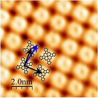
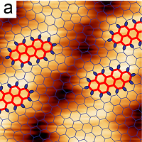 STM observation of molecule-induced band gap opening in single layer graphene Scanning Tunneling Microscopy (STM), Spectroscopy (STS), and manipulation studies were performed on an ordered self-assembled monolayer (SAM) of N,N’-bis(1-hexylheptyl)perylene-3,4:9,10-bis(dicarboximide) molecules on epitaxial graphene on hexagonal silicon carbide – SiC(0001). Four novel aspects of the molecular SAM on graphene are presented. Molecules adsorb in both armchair and zig-zag configurations, giving rise to six orientations of the molecular layer with respect to the underlying substrate. The interaction between the molecules and the graphene surface shifts the LUMO towards the Fermi Level, inducing a charge transfer and the opening of a band gap in the graphene, with the LUMO inside. This decouples the LUMO from the surface rendering it is invisible in the dI/dV spectroscopy. The HOMO only becomes visible at short tip-surface distances, as its energy lies within the band gap of the SiC substrate. Finally, the observed molecular defects are very particular, being composed exclusively of molecular dimers. These molecular dimers have a stronger interaction with the graphene than other molecules. STM observation of molecule-induced band gap opening in single layer graphene Scanning Tunneling Microscopy (STM), Spectroscopy (STS), and manipulation studies were performed on an ordered self-assembled monolayer (SAM) of N,N’-bis(1-hexylheptyl)perylene-3,4:9,10-bis(dicarboximide) molecules on epitaxial graphene on hexagonal silicon carbide – SiC(0001). Four novel aspects of the molecular SAM on graphene are presented. Molecules adsorb in both armchair and zig-zag configurations, giving rise to six orientations of the molecular layer with respect to the underlying substrate. The interaction between the molecules and the graphene surface shifts the LUMO towards the Fermi Level, inducing a charge transfer and the opening of a band gap in the graphene, with the LUMO inside. This decouples the LUMO from the surface rendering it is invisible in the dI/dV spectroscopy. The HOMO only becomes visible at short tip-surface distances, as its energy lies within the band gap of the SiC substrate. Finally, the observed molecular defects are very particular, being composed exclusively of molecular dimers. These molecular dimers have a stronger interaction with the graphene than other molecules. |
Article : H. Yang, A.J. Mayne, G. Comtet, G. Dujardin, Y. Kuk, L. Stauffer, Ph. Sonnet, S. Nagarajan, A. Gourdon, "STM imaging, spectroscopy & manipulation of a self-assembled PTCDI monolayer on epitaxial graphene", Phys. Chem. Chem. Phys. 15, 4939 (2013)
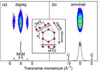
 Quantum Interference Channeling at Graphene Edges. Electron scattering at graphene edges is expected to make a crucial contribution to the electron transport in graphene nanodevices by producing quantum interferences. Atomic-scale scanning tunneling microscopy (STM) topographies of different edge structures of monolayer graphene show that the localization of the electronic density of states along the C-C bonds, a property unique to monolayer graphene, results in quantum interference patterns along the graphene carbon bond network, whose shapes depend only on the edge structure and not on the electron energy. Quantum Interference Channeling at Graphene Edges. Electron scattering at graphene edges is expected to make a crucial contribution to the electron transport in graphene nanodevices by producing quantum interferences. Atomic-scale scanning tunneling microscopy (STM) topographies of different edge structures of monolayer graphene show that the localization of the electronic density of states along the C-C bonds, a property unique to monolayer graphene, results in quantum interference patterns along the graphene carbon bond network, whose shapes depend only on the edge structure and not on the electron energy. |
Article : H. Yang, A.J. Mayne, M. Boucherit, G. Comtet, G. Dujardin, Y. Kuk, "Quantum Interference Channeling at Graphene Edges", Nano Letters 10, 943 (2010)
Dans la même rubrique :